

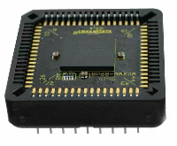
PLCC68 series are very small stamp size FPGA & CPLD Module.
They are designed to be used with 68-pin PLCC socket, so it's very convenient to utilize on universal boards.
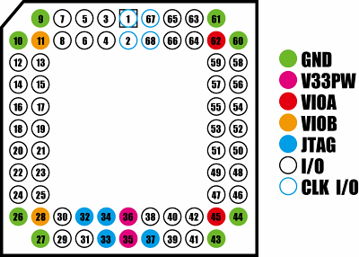
PLCC68 series require only single 3.3V power supply. Pin assignments are same in all series. Vcco output driver supply is separated in two banks (A and B, 25 I/Os each).
These features are common for all series regardless of its FPGA/CPLD type.
|
|
|
|
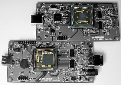
Usage Example |
INTEL
| No | Description | FPGA / CPLD | Series | Image | Features | DOC |
|---|---|---|---|---|---|---|
| 1 | MAX II PLCC68 CPLD Module | EPM240F100C5N EPM570F100C5N |
AP68-01 |  |
|
|
| 2 | MAX V PLCC68 CPLD Module | 5M570ZF256C5N | AP68-02 |  |
|
|
| 3 | Cyclone III PLCC68 FPGA Module | EP3C5U256C8N EP3C10U256C8N |
AP68-03 |  |
|
|
| 4 | Cyclone III PLCC68 FPGA Module | EP3C25U256C8N | AP68-04 |  |
|
|
| 5 | Cyclone V PLCC68 FPGA Module | 5CEBA4U15C8N | AP68-06Z |  |
|
|
| 6 | Cyclone V PLCC68 FPGA Module | 5CEBA4U15C8N | AP68-07 |  |
|
|
| 7 | MAX 10 PLCC68 FPGA Module | 10M08SAU169C8GES | AP68-08 |  |
|
|
| 8 | Cyclone 10 LP U256 PLCC68 FPGA Module |
10CL006YU256C8G 10CL010YU256C8G 10CL016YU256C8G 10CL025YU256C8G |
AP68-09 |  |
|
|
| 10 | MAX 10 DCU324 PLCC68 FPGA Module | 10M08DCU324I7G 10M16DCU324I7G |
AP68-10 |  |
|

AMD (XILINX)
| No | Description | FPGA / CPLD | Series | Image | Features | DOC |
|---|---|---|---|---|---|---|
| 1 | Spartan-6 PLCC68 FPGA Module | XC6SLX16-2CSG225C | XP68-01 |  |
|
|
| 2 | Spartan-3AN PLCC68 FPGA Module | XC3S200AN-4FTG256C | XP68-02 |  |
|
|
| 3 | Spartan-6 PLCC68 FPGA Module | XC6SLX45-2CSG324C | XP68-03 |  |
|
|
| 4 | Artix-7 PLCC68 FPGA Module | XC7A15T-1CSG324C XC7A35T-1CSG324C XC7A50T-1CSG324C XC7A75T-1CSG324C XC7A100T-1CSG324C |
XP68-05 |  |
|
|
| 5 | Spartan-7 PLCC68 FPGA Module | XC7S25-1CSGA324C XC7S50-1CSGA324C |
XP68-06 |  |
|
|
| 6 | Spartan-7 PLCC68 FPGA Module | XC7S25-1CSGA225I | XP68-07 |
|
Key Features
- 50 I/Os (4 I/Os: assigned to clock preferentially)
- 3.3 V single power supply operation (auxiliary power for FPGA/CPLD is built-in)
- Mountable on 68pin PLCC socket
- Separable VCCO (VIO(A)/VIO(B), MAX 3.3 V)
- JTAG signal (TCK, TMS, TDI, TDO) is available
- Common pin assignment for all PLCC68 series
- Non-use of 6 Restricted substances of RoHS directive
- MADE IN JAPAN
Application Note
[ ]
